 Support l'X
 An optical platform for fabricating and studying nanostructures
 The LSI conducts fundamental research on nanostructures using optical methods, with contributions from students from bachelor and Ingénieur Polytechnicien programs
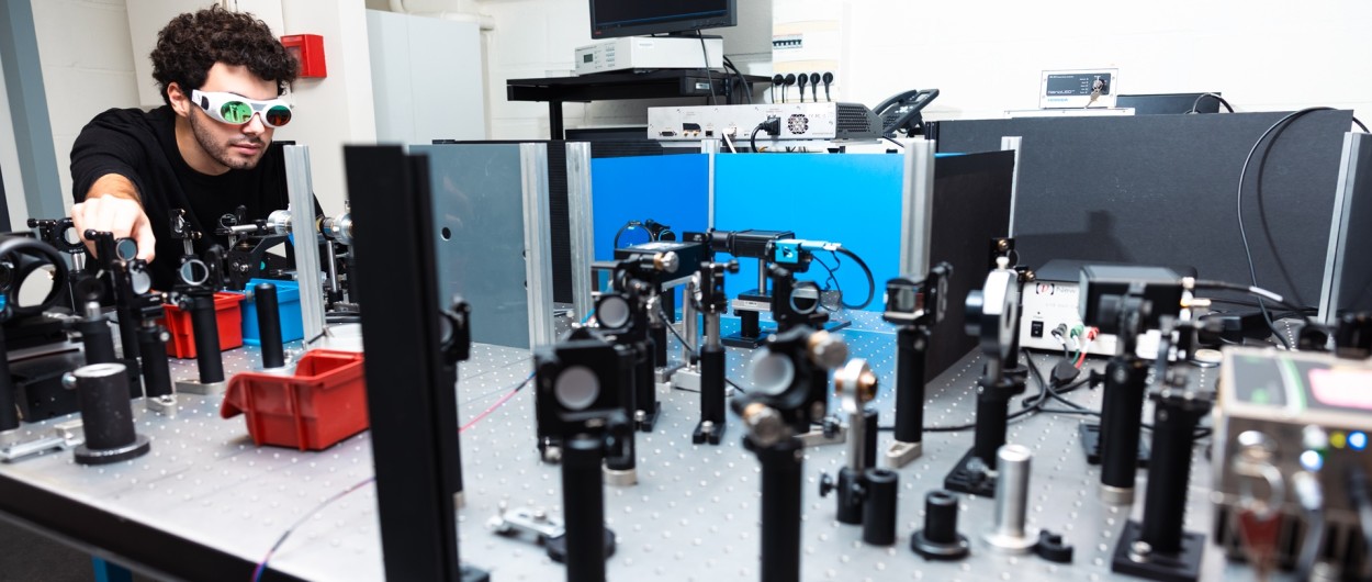
Using ultra-fast laser beams, a team from the Irradiated Solids Laboratory (LSI*) has designed an experiment that allows both the creation of nanometric cavities in metal films and their study using several advanced microscopy techniques. The results have been published in the journal Physical Review Letters (PRL).
Sunlight passing through a magnifying glass can set a sheet of paper on fire. Similarly, a focused laser beam can cut certain materials. This principle is already widely used on an industrial scale. But the fineness of laser beams also makes it possible to etch nanometer-sized patterns.
While these “laser lithography” techniques already exist, a collaboration led by a team at the LSI has gone further by combining the fabrication of nanostructures in thin metal films and their in situ characterization on a single platform. Ultimately, this could lead to faster and cheaper nanofabrication technologies.
The light beam used for the experiment is produced by a laser that creates ultra-short pulses, on the order of a millionth of a billionth of a second (i.e., a femtosecond).
A 3-in-1 platform
The researchers created cavities by separating a metal film (such as nickel, iron, or a multilayer structure) from an insulating substrate. “By changing the size and characteristics of the femtosecond laser beam, it is possible to shape the structure, and in particular the curvature of the cavity,” explains Vasily Temnov, a physicist at LSI, who worked with two Bachelor's students from École Polytechnique on a Projet de Recherche en Laboratoire (PRL) research project, Akira Barros and Aditya Swaminathan.
Three methods for characterizing these structures were implemented in the same experiment: an interferometric microscopy technique, which allows the formation of these structures to be observed; a photoacoustic microscopy technique, used in particular to study the vibration of the cavities; and magnetoplasmonic microscopy. The latter technique uses a laser beam and a magnetic field to probe the collective states of electrons, known as plasmons, which are very difficult to observe in these nanostructures. This is the first experiment to successfully combine all these aspects.
This work paves the way for fundamental research into the excitation of various quasiparticles (phonons, plasmons, magnons, etc.) in these nanometric structures, before considering possible applications such as pressure or magnetic field sensors integrated onto chips.
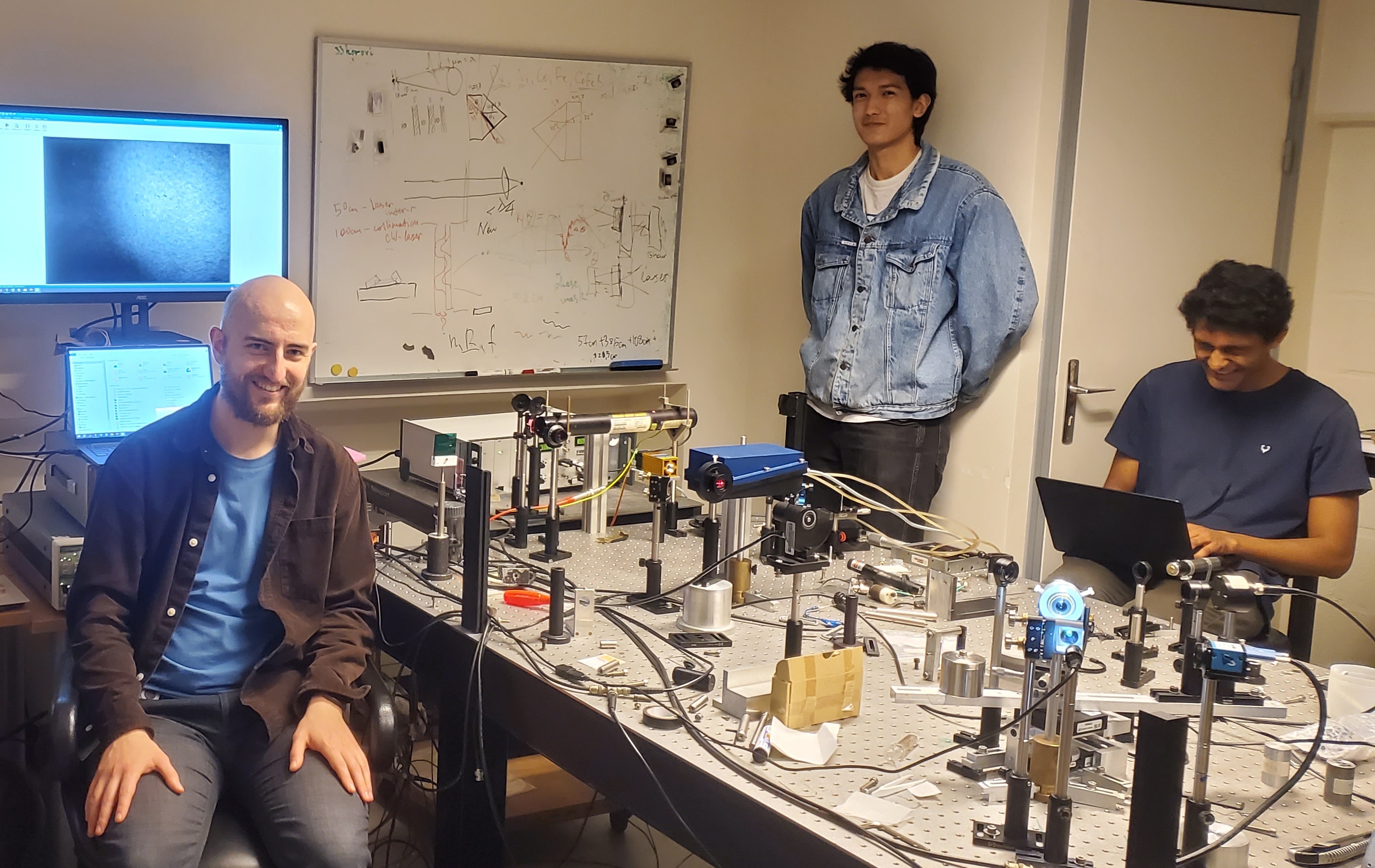
From left to right, Pavel Varlamov, Akira Baros, and Aditya Swaminathan, first authors of the article.
Publication reference:
Femtosecond-Laser-Delamination Cavities for Resonant Acousto-Magneto-Plasmonics P. Varlamov, A. Barros, A. Swaminathan, et al., Physical Review Letters, 2025 DOI: https://doi.org/10.1103/99sl-xxb2
*LSI: a joint research unit CEA, CNRS, École Polytechnique, Institut Polytechnique de Paris, 91120 Palaiseau, France